Solar-powered five-leg inverter-driven quasi-dynamic charging for a slow-moving vehicle
 Yuvaraja Shanmugam1,
  R. Narayanamoorthi1*,
  Pradeep Vishnuram1,
  Dominic Savio1,
  Arvind Yadav2,
  Mohit Bajaj3,4*,
  Ali Nauman5*,
  Tahir Khurshaid6* and
  Salah Kamel7*
- 1Electric Vehicle Charging Research Centre, Department of Electrical and Electronics Engineering, SRM Institute of Science and Technology, Chennai, India
- 2Department of Electrical Engineering, GLA University, Mathura, India
- 3Department of Electrical Engineering, Graphic Era (Deemed to be University), Dehradun, India
- 4Applied Science Research Center, Applied Science Private University, Amman, Jordan
- 5Department of Information and Communication Engineering, Yeungnam University, Gyeongsan, Republic of Korea
- 6Department of Electrical Engineering, Yeungnam University, Gyeongsan, Republic of Korea
- 7Electrical Engineering Department, Faculty of Engineering, Aswan University, Aswan, Egypt
Road transport is becoming increasingly electric as it becomes more environmentally friendly. A green transportation system includes solar arrays along the roadside, encouraging the eco-friendly EV charging system. This paper proposes a road-side photovoltaic system to charge the batteries of slow-moving electric vehicles using a five-leg inverter. The five-legged inverter, which utilizes a stand-alone PV system to drive the charging pads, enhances the probability of achieving the sustainability goal. The limitations of the conventional H-bridge inverter, such as its more prominent design and higher number of switches or straightforward design and restricted power level, are addressed by this converter. The proposed 3.3 kW, 85 kHz inverter energizes the four transmitter pads while a receiver pad moves over the transmitter pads and inductively extracts the power. The d.c.-d.c. converter is used to feed the power to the proposed inverter. The P and O-based MPPT algorithm with a tuned PI controller is used to generate the driving pulses of the d.c.-d.c. converter. The signals are generated based on the voltage and current output of the solar panel output. This control algorithm ensures the stability of the system output response. Additionally, the tuned d.c.-d.c. converter achieves maximum efficiency independent of the load resistance. The system maintains constant power transfer profile concerning load resistance variations. The 520*520 mm Double D-pad transmits the power, while the series-series compensation network assists the charging pads in achieving resonance. The developed systems’ nominal charging voltage and current are 144 V, 20 A, with an equivalent battery resistance of 7.2 Ω.
1 Introduction
In recent days, climate change has become an urgent issue, and many countries have pledged to limit temperature increases to 1.5°C or less. All countries must also reduce greenhouse gas emissions. The emissions must be reduced by 45% by 2030. Developing countries are encouraged by the Paris agreement to achieve net-zero emissions in their regions (The Paris Agreement United Nations, n.d.). The transportation sector is one of the major contributors to greenhouse gas emissions. Green transportation includes EVs, such as plug-ins and battery-electric cars, helping to reduce emissions. Every year, EV sales increase rapidly. As the EV market grows, more batteries and related materials are needed (The Global Electric Vehicle Market In, 2022—Virta, 2022). Bulk battery requirements are one of the major considerations when designing an EV. A limitation of EV market growth is their limited driving ranges because of large battery requirements. EV battery recharging infrastructure development must suit the development of on-road EVs. A wireless charging system is proposed to overcome the drawbacks of wired charging, such as the need for bulky mechanical conductors, and driver dependency. Wireless charging for EVs majorly uses IPT technology to charge storage devices. It reduces the maximum demand for driver dependency on the charging process (Mahesh et al., 2021). An IMC system can extend the range of an EV with a reduced battery pack. A vehicle is being charged by an IMC system while in driving mode. A key requirement of the IMC system is lateral and longitudinal misalignment tolerance, the significant air gap between pads, affordable costs, low surrounding temperatures, and low mechanical vibrations (Choi et al., 2015). Charging couplers, compensation circuits, and power converters are the main components of the IMC system. A charging coupler consists of a transmitter and receiver. A transmitter pad is mounted along the roadside, and a receiver pad is mounted under the vehicle. When a vehicle is positioned over the transmitter pad, the receiver pad will energize the vehicle’s battery. When both transmitter and receiver pads are properly aligned, the maximum power is transferred between them. The types of transmitter pads are lengthened track and segmental track (Farajizadeh et al., 2020). Despite the simplicity of energizing lengthened track, the uncoupling part of the coil causes high power losses. So, the segmented continuous charging pad track is preferred in roadway-powered transportation (Laporte et al., 2019). The non-polarized and polarized pads are the main classification of charging pads (Rahulkumar et al., 2022). The Stellantis demonstrated the charging of the EVs by DWPT technology successfully. The driver does not need to stop the vehicle from charging the batteries. The advantages of the DWPT system are reduced power losses, direct integration of renewable sources, thinner cables than a.c. distribution, and able to use aluminum cables to distribute current, which affects cost reduction (Arena del Futuro Demonstrates Capability of Dynamic Inductive Recharging Technology for Electric Vehicles Stellantis, 2022). The basic representation of the PV-integrated DWPT system is represented in Figure 1.

FIGURE 1. Representation of PV-integrated DWPT system.
Integration of a renewable energy source with the IMC system upgrades the range of green transportation. The solar-based road surveillance system (Celik & Kusetogullari, 2010), and solar-based e-bike charging system (Mouli et al., 2020) encourage green transportation. The long national highways are an enormous source of solar energy. The maximum solar energy can be extracted along the roadside. Many countries installed solar panels along the roadside to generate power, and that generated power is transferred to utilizers through the long grid (Huang et al., n.d.; Indian highway to host 250 MW solar plant—pv magazine International, 2022). The first 1-km long 2,800 m2 solar road is developed in Normandy, France (Zhou et al., 2021). The power quality issues raised by the IMC system in a utilization grid can be reduced by utilizing roadside solar power. Figure 2 represents the overall circuit diagram of the proposed DWPT system. Table 1 represents the existing inverter topologies.
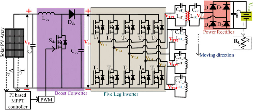
FIGURE 2. Circuit description of the proposed DWPT system.
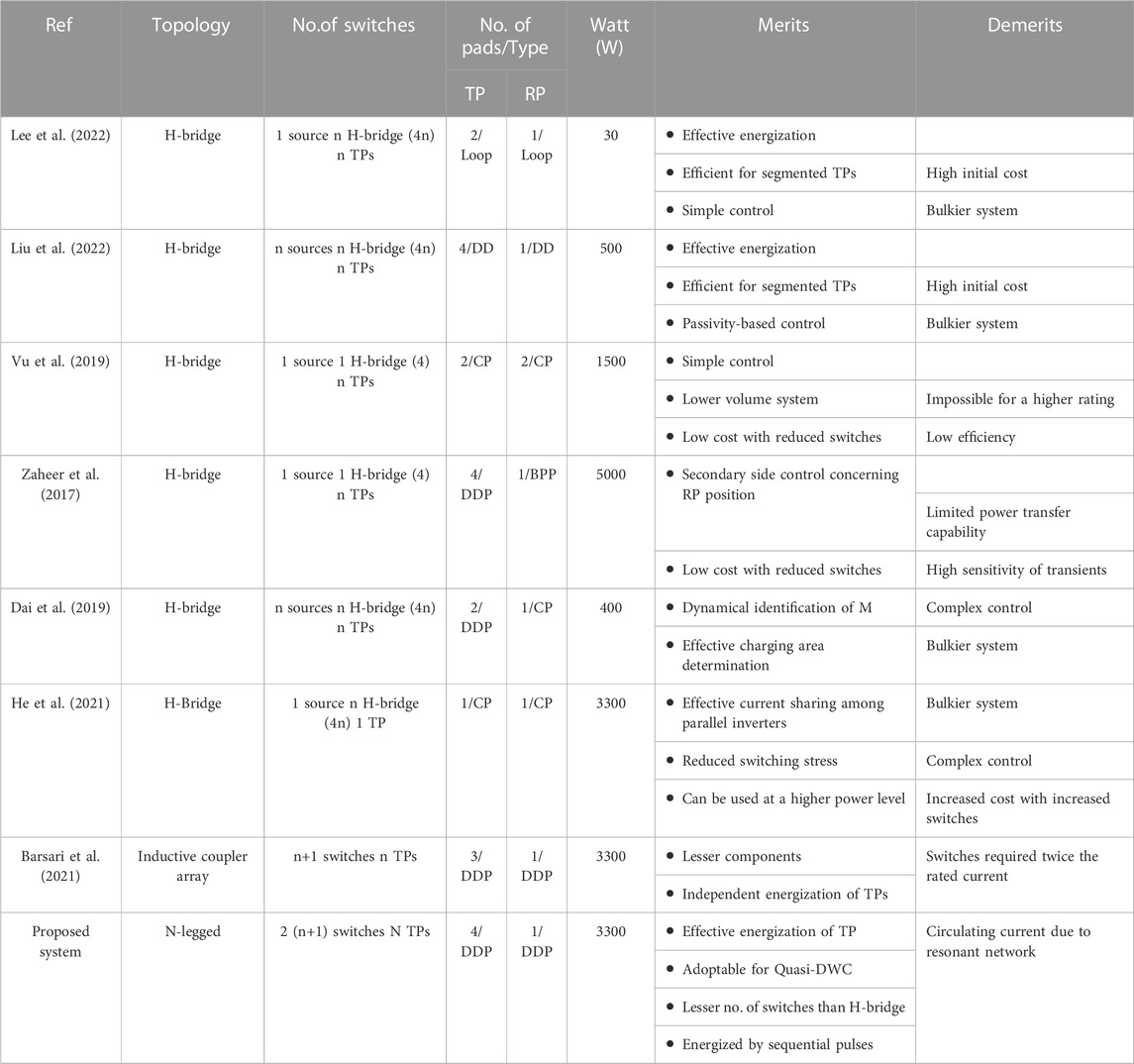
TABLE 1. Existing wireless charging inverter topologies.
The 3.3 kW Ablytek 6MN6A270 PV array, which has an open-circuit voltage of 38.63 V and a short circuit current of 9.34 A, is used for simulation studies. The polarized DDP is used in this paper to transmit the power due to its better misalignment tolerance for lateral and longitudinal movement. Additionally, it provides a better charging zone than a non-polarized rectangular pad (Yang et al., 2021). A researcher from Qualcomm verified the merits of DDP experimentally over the rectangular and solenoidal pad with the help of a 3.3 kW and 2.2 kW charging system (Ombach et al., 2015). A KRRI demonstrated the 1 MW 128 m long track DWPT system with 82.7% efficiency for a HEMU-430x high-speed train. A 5*200 kW inverter is used to energize the five transmitter pads (Kim et al., 2015). KAIST developed the 100 kW DWPT system for moving EVs with an example of OLEV. The system provided 80% power transfer efficiency with a 26 cm air gap. The elongated track was energized by the five-pickup mounted beneath the OLEV with the help of two modular inverters (Shin et al., 2014). The multiple modular inverters manufactured in larger quantities designed to power a single receiver simultaneously are an efficient way to upgrade the IPT system’s power capacity with the demand for high-power applications. This paper proposes a five-legged inverter driven by a solar-integrated boost converter. This five-legged inverter energizes the four transmitter pads. The series-series compensation network reduces the input impedance variations concerning the load changes (Shanmugam et al., 2022). A slight change in the output current of the power inverter leads to a significant change in the transmitter current in a parallel-parallel compensation network. So, it is hard to control the transmitter current effectively while using this network (Kim et al., 2015).
2 Overall system design
2.1 Boost converter with PV arrays
Figure 3 represents the MPPT-controlled PV integrated boost converter. The MPPT-based boost converter is used to regulate the output of the PV arrays (Singaravel & Daniel, 2015). The driving signal of the d.c.-d.c. converter’s switch is generated relevant to the PV arrays voltage (V) and current (I) based on the P and O MPPT algorithm (Hohm & Ropp, 2000). The P and O MPPT algorithm is used for its ease of control, and the parameters are adjusted concerning the tuned PI controller. The voltage limits of PV arrays have controlled within 90 V–100 V. The driving signal is automatically adjusted to the variations of specific parameters such as load, temperature, and irradiation to maintain the constant output voltage. Four parallel strings form the 3.3 kW with three series-connected modules per string. The PV arrays’ open circuit voltage (Vo.c.), and short circuit current (Is.c.) are 116 V and 36 A, respectively. The purpose of an MPPT control is to obtain the maximum efficiency of the PV arrays. The voltage of the PV array depends on the temperature and irradiation of the Solar System. Since the proposed system is dynamic charging, the system will supply constant voltage to the charging load. The efficiency of the MPPT is defined by
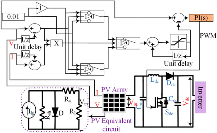
FIGURE 3. Representation of MPPT-controlled PV integrated boost converter.
Where Pactual is the actual power generated by the PV panels with MPPT control, and Pmaximum is the maximum power produced by the PV panels for given solar irradiance (W/m2) and panel temperature (0C). The traditional I-V curve of the PV arrays can be obtained from the Eqs. 2–5 by neglecting internal shunt resistance (Rsh) (Koutroulis et al., 2001).
Where, Iout output current of the solar cell, Ilight current generated by light, Ireverse reverse saturation current of the solar cell, q electronic charge, k Boltzmann’s constant, T temperature of the solar cell in 0C, Vout output voltage of the solar cell, Rs series resistance, Isaturation saturation current of the solar cell at Tr, Tr reference temperature 28.03°C, EGO silicon band gap, B = A = 1.92 ideality factors, Is.c. solar cell short circuit current, KI 0.0017 temperature co-efficient of short circuit current, λ solar cell irradiation at W/m2. The P and O algorithm is framed with the help of a tuned PI controller (Mohamed et al., 2021), and the controller is used to generate the driving pulses to the semiconductor switch of the boost converter with a switching frequency (fs_boost) of 10 kHz. The converter output voltage depends on the output of the PV array. The duty cycle of the converter is set by 0.712. So, the converter nearly 3.4 times multiplies the input voltage. The input capacitor (Cin) is cautiously designated to provide the constant voltage to the converter. It supplies the constant voltage to the inverter for a particular instant. The dynamic charging system operated with these inconsistent constant voltage variations. The MPPT controller requires a voltage and current signal from the PV arrays, which maximizes the power. Since the proposed converter is a stand-alone PV system which is used road-side installed PV panels. In order to maintain the supply as constant irrespective of the irradiation level, we need to have an energy storage unit coupled with the PV. Considering the original concept is on the wireless charging section, the voltage balancing capacitor is connected at the output side of the PV source for the simulation and experimental analysis to test the proposed system. Wireless charging units will receive constant energy supplies from an energy storage system when implemented in real-time.
The increases in the load resistance affect the output voltage of the converter. Figures 4A–C represents the response of the boost converter, and 4c represents variations of voltage gain concerning load resistance. The elements of the boost converter are designed as follows (Umanand, 2009)
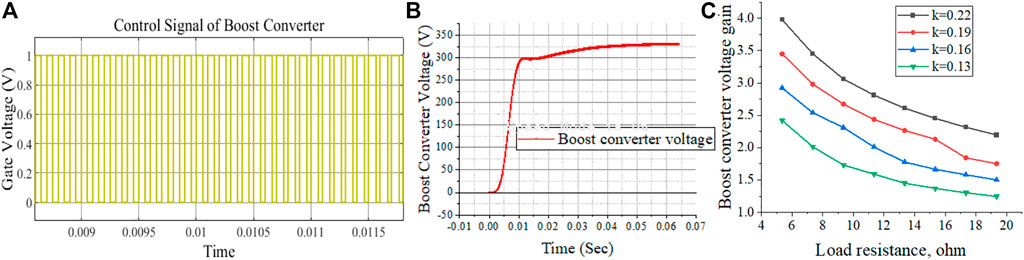
FIGURE 4. Boost converter waveforms (A) PWM signal (B) Output voltage (C) Voltage gain concerning the load resistance.
2.2 Five-legged inverter
In general, an HPHFI is used to control the energization and de-energization process of the transmitter pads. The standard operating frequency of the HPHFI is suggested to be 85 kHz by SAE J2954 (SAE International, 2020). The roadside-embedded N number of transmitter pads can be driven by a single H-bridge inverter (Vu et al., 2019) or an N number of H-bridge inverters (Lee et al., 2022). The N-legged converter is proposed (Farajizadeh et al., 2020) to drive the N-1 closely spaced transmitter pads. The effect of cross-coupling due to adjacent pads can be minimized by an additional inductor connected serially to the transmitter pads. The instantaneous output voltage of the inverter can be given by (Rashid, 2004).
The different modes of operation of a PV-integrated five-leg inverter are represented in Figure 5. The output of the boost converter is fed to the five-legged inverter and the adjacent pair of legs is operated as a conventional H-bridge inverter to energize the transmitter pads. There are 10 power MOSFET switches from T1 to T10 that are used in the five-leg inverter. The MOSFET switches T1-T4, T3-T6, T5-T8, and T7-T10 are used to drive the TP1, TP2, TP3, and TP4 respectively. The driving pulses of the switches generated depend on the position of RP. The node voltages of each leg of the five-leg inverter are VL1, VL2, VL3, VL4, and VL5. The TPs are energized based on the position of the receiver pad (RP). The leg voltages VL1 and VL2 are fed to TP 1 when RP is positioned over it. The adjacent leg switches are involved in the energization process when the RP is moving horizontally. The moving speed of the RP is based on the conduction period of the switches. When the RP is positioned over TP 1, the path of the power flow as represented in Figure 5 is Vd.c.+-T3-VL2-LsT_1-CcT_1-VL1-T2-Vd.c.− and Vd.c.+-T1-VL1-CcT_1-LsT_1-VL2-T4-Vd.c.− in a mode 1. The adjacent leg switches engage in the process of charging the TP as it moves along the charging track. The driving pulses of the proposed inverter are represented in Figure 6. The total mutual inductance in each mode is the summation of the mutual inductance by the cross-coupling effect and trans-coupling effect (Farajizadeh et al., 2020). The cross-coupling is the effect of adjacent side pads and trans-coupling is the effect of opposite side pads on the live charging pad. The equivalent circuit to explain the trans and cross-coupling is represented in Figure 8A. The effect of cross-coupling effect can be reduced by embedding the TPs at a proper distance. When RP is positioned over TP1, the total mutual inductance of the TP1 (MT1) is defined by
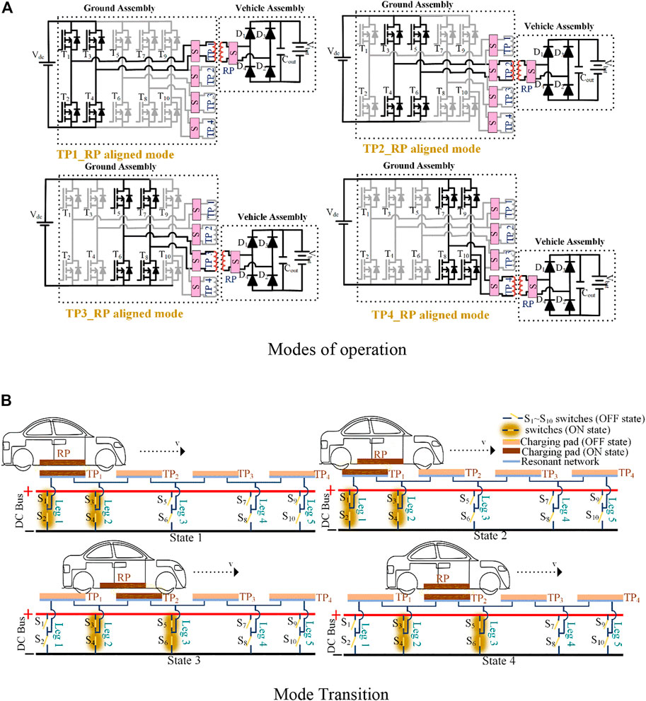
FIGURE 5. Modes of operation of a five-leg inverter. (A) Modes of operation, (B) Mode Transition.
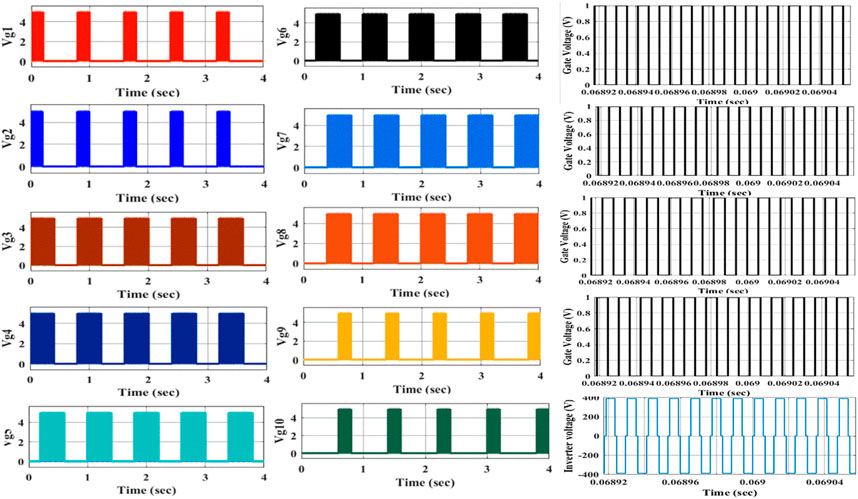
FIGURE 6. PWM patterns proposed inverter.
In this paper, the phase-shifted PWM signal is fed to the inverter’s switches represented in Figure 6. The inverter pulse of the upper switch is fed to the lower switch in each leg. The firing delay, α is introduced between the upper switch of leg 1 and the lower switch of leg 2 in an inverter. The driving pulses are triggering the respective switch by following the position of the RP. Once the presence of RP is sensed nearer to the TP1 manually, the driving signals of the switches of five leg inverter are generated in sequence with a particular interval. Based on the sequence interval the RP has to move on the TPs. The minimum dead time is provided during the leg-to-leg transition. The dead time is nothing but time taken to shift the energization pulses from mode 1 to mode 2. The open-loop control is performed by spartan FPGA kit toggle switch. The level of power transfer concerning to the flux linkage during longitudinal movement. During the misalignment, the power transfer efficiency is low compare to the fully aligned condition. The resonant network improves the power transferring profile during the misalignment. The uniform power transfer profile will be maintained by allowing the optimum spacing between the transmitter pads. The operating frequency of the driving pulses is 85 kHz (SAE International, 2020). The 85 kHz triangle pulses are compared with the d.c. line and the driving pulses of the proposed inverter are generated. The soft-switching of the five-leg inverter is difficult due to resonant effect of the charging pads. Since the proposed converter used for a dynamic charging. The reactance parameters of the charging pads and resonant capacitor inconsistent at dynamic charging process. During the mode transition, the circulating current in the charging pad never reaches zero due to its inductive nature. The transmitter pads are placed at certain distance to maintain a uniform power transfer profile. A Low magnitude current passes through the switches due to resonant network during the transition. The protection circuit will protect the switches from overcurrent and overvoltage during transition.
The variations of inverter voltage gain and current concerning the load resistance and temperature of the PV arrays are represented in Figure 7. The voltage gain of the inverter is decreased when the load resistance is increased. The current flowing through the inverter (ITP) increases the load resistance proportionally. The rated power of HPHFI decreases as the temperature of the PV array increases.
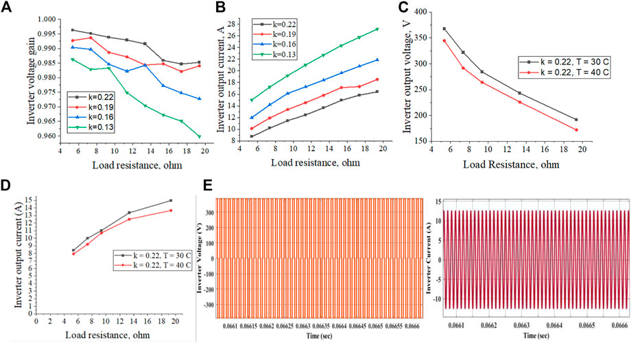
FIGURE 7. Response of HPHFI (A) Load resistance Vs. Voltage gain (B) Load resistance Vs. Leg to Leg inverter current (C) Load resistance Vs. Output voltage (with different temperature) (V) (D) Load resistance Vs. Inverter output current (with different temperature) (E) Current and a voltage waveform of the inverter.
A proposed five-leg inverter controls the energization of the transmitter pads. A spartan-6 FPGA kit triggering the switches of combinational legs. In this proposed prototype, the four transmitters are connected to the inverter. The transmitter pads are arranged with the particular distance to minimize the cross-coupling inductance between them and to transmit uniform power to the receiver. Here, the TPs are spaced with a 570 mm horizontal distance, and the RP is moved over the TPs at certain velocity. The spacing between the TPs are considered to maintain the uniform power transfer profile. While moving the RP horizontally, the induced voltage across the RP will vary by induction principle. The current flowing through the RP unable to reach zero position due to short period, i.e., the RP will get energization by immediate TP. The TP1 receives the energization signal from leg 1 and leg 2 for a period sec and after that adjacent leg 3 will be involved in the charging process and the power is transferred by TP2. When the RP moves from the top of TP1 to the top of TP2, the leg 1 eliminated from the process and leg 3 engaged the energization process. The leg 1 and leg 3 are triggered parallelly. T1 and T2 switches get turned-off and T5 and T6 switches gets turned-on. This operation will continue concerning to the movement of RP. While moving over the gap of two transmitter pads, RP receives considerable power which less than fully aligned condition. The series resonant network is used to achieve the maximum power during misalignment condition.
2.3 Compensation network
The compensation network is used to maximize power transfer efficiency, minimize VA rating, and provide excessive misalignment tolerance and bifurcation tolerance (Patil et al., 2017) (Narayanamoorthi et al., 2019). Our proposed system uses the series-series network to maintain the unity power factor at resonant frequency conditions, ensure the smooth switching transitions, and maintain the transmitter capacitance independent of coupling coefficient (k) variations. And also, it is used to manage the track voltage within allowable limits (Shevchenko et al., 2019). The equivalent circuit of the compensation network is represented in Figure 8B.
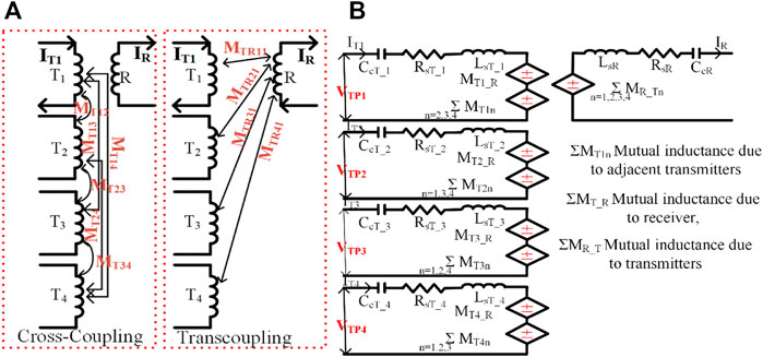
FIGURE 8. (A) Representation of cross-coupling and trans-coupling (B) Equivalent circuit of the compensation network.
The trans-coupling mutual inductances are mentioned as MT1_R to MT4_R and cross-coupling mutual inductances are mentioned as
In Figure 8 the reflected impedance from the receiver side to the transmitter side (Zr) is (Aditya, 2016)
and the total input impedance (ZT_in) from the TP side is
The self-inductance of the receiver pad is given by
Where, the range of secondary quality factor Qs, is usually chosen between 2 and 10. And also, the greater value of Qs makes the system hard to tune, and a lesser value of Qs will introduce harmonics in an output waveform. The bifurcation can be avoided by selecting a k value lesser than critical coupling, kc.
The value of self-inductance of the transmitter pad is calculated depending on the fixed value of k. The calculated Kc with the value of Qs = 4 is 0.248. So, the finalized value of k is 0.22. The equivalent a.c. value of the d.c. load resistance with the bridge rectifier and a capacitive filter is (Aditya, 2016)
Where V0 is the output voltage of the system and P0 is the output power of the system. Then, the calculated receiver pad self-inductance concerning Qs = 4, P0 = 2880 W, V0 = 144 V is 55.1 μH. The mutual inductance (M) of the charging pads can be calculated from Eq. 24
The calculated transmitter and receiver side current for the 3.3 kW system is 11 A and 19.51 A respectively. Concerning these values, the calculated M is 24.43 μH. Once the k, M, and LsR values are calculated, the transmitter pad self-inductance is given by
From the resonant frequency and the self-inductance of the transmitter and receiver pad, the value of transmitter side and receiver side compensation capacitor values are given by
The theoretical efficiency of the compensation network is (Patil et al., 2017)
As per (Eq. 27), the obtained theoretical efficiency with the wounded litz conductor is 98%. Efficiency is calculated with the resistance values of 1050 strands (0.1016 mm diameter) and a 5.2 mm diameter conductor.
2.4 Charging coupler
DWPT system relies heavily on charging couplers. The essential parts of the charging couplers are the transmitter pad (TP), receiver pad (RP), core, and shielding. The transmitter pad transfers the power through an air medium and the receiver pad extracts the power from TP. The considerations of the charging couplers are the distance between pads, charging power, coupling inductance parameters, and misalignment tolerable range (Yuvaraja et al., 2022) (Narayanamoorthi & Juliet, 2019). The different classifications of charging couplers are lumped or distributed, polarized or non-polarized, and single-sided flux or double-sided flux. The efficiency of the charge couplers in a DWPT system can be affected by the product of quality factor, Q, and co-efficient of coupling, k. The Q value can be increased by designing a charging pad with large self-inductance and low series resistance at a high range of frequency (Patil et al., 2017). The k value can be increased by placing the ferrite bars or plates with the charging pads. The polarized single-sided flux DDP (Budhia et al., 2013) is developed to increase the horizontal misalignment tolerance level higher than non-polarized pads such as circular, flux-pipe, rectangular, and square. Additionally, DDP has better leakage performance than square and rectangular. The flux path height of the DDP is half of the length of the pad resulting in higher k, improved no-load Q, and reduced leakage flux from the back of the pad (Patil et al., 2017). In this paper, the transmitter and receiver pad have 35 turns and 10 turns respectively. The outer diameter of the charging pads is equal to obtain maximum efficiency (Aditya, 2016). The cited paper provides the analysis of the various combinations of the TP-RP concerning the coupling efficiency. The dimensions of the charging pads and ferrite bars are represented in Figure 9.
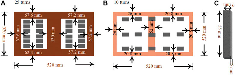
FIGURE 9. Dimensions of (A) transmitter pad (B) receiver pad (C) ferrite core.
The inductance of the DDP can be calculated by determining the self-inductance of the individual conductor segments and mutual inductance between adjacent and opposite side conductor segments. The direction of the current is the same in adjacent conductors and opposite in return path conductors. The self-inductance of the straight cylindrical conductor (L) with the ‘l’ length ‘r’ radius is (Rosa and Grover, n.d.)
Mutual inductance between two adjacent parallel conductors with a distance of d is
And, the mutual inductance between segments with opposite current flowing directions is (Formul812871912169169unse, n.d.)
where μ is the permeability of the conductor.
The skin effect of the conductor with σ is given by (Grover and Instrument Society of America, 1981)
Since, the mutual inductance of the parallel conductors is positive for the same direction of current flow and negative mutual inductance for the opposite direction of current flow (Greenhouse, 1974). The total inductance, LT of the pad is given by the summation of all the self-inductances and mutual inductances.
When the parallel conductors are different lengths of m + p, m, the mutual inductance between the conductors i, j is
When the receiver pad is moving horizontally, the direction of the current is changing in the aligned segments and the mutual inductance becomes negative. The movement of the RP to denote the reason for negative mutual inductance and k is represented in Figure 10.
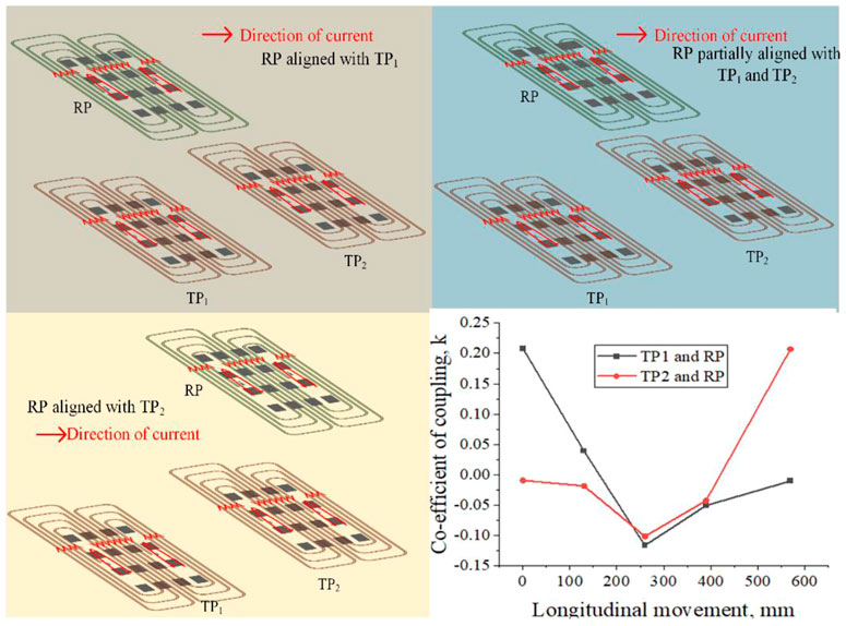
FIGURE 10. Variations of k concerning the misalignment.
Based on the analysis, the designed coil dimensions are represented in Figure 9. The self-inductance of the simulated TP and RP is 223.8 μH and 55.082 μH respectively. The air gap between charging pads is 100 mm. The dimensions of the ferrite bar are mentioned in Figure 8C. The number of ferrites used with TP and RP is 30 and 15 respectively with a 55*45*9 mm cross-section. The 85,000 kHz, 11A current is passed through the transmitter pads alternatively concerning the movement of RP. The ratio of the d.c. resistance to a.c. resistance of the Litz wire is given by (Litz wire technical information, NEW, 2003)
Where H is an isolated strand’s resistance ratio and it may have values of 1.0000, 1.0003, 1.0007, 1.0012, 1.0021, 1.0034, 1.005 for the X values of 0, 0.5, 0.6, 0.7, 0.8, 0.9, 1.0 respectively. The value of X for the copper wire can be calculated by
Where Dwire is the diameter of the wire in mils, fMHz is the frequency in MHz. The eddy current basis factor, G can be obtained by
Where f is an operating frequency, N is the number of strands in the cable, Dstrands is the diameter of the individual strands over the copper in inches, Dcable is the diameter of the finished cable over the strands in inches and K is the constant depending on N which is having the values of 1.55, 1.84, 1.92 and 2 for the values of 3, 9, 27 and infinity respectively. The a.c. strand loss of the 5.2 mm diameter, 38 AWG, 1050 strands conductor is 3.192 W. The resistance of the TP and RP is 28.4 mΩ and 13.38 mΩ. The simulated results for various misalignment conditions are represented in Figure 11.
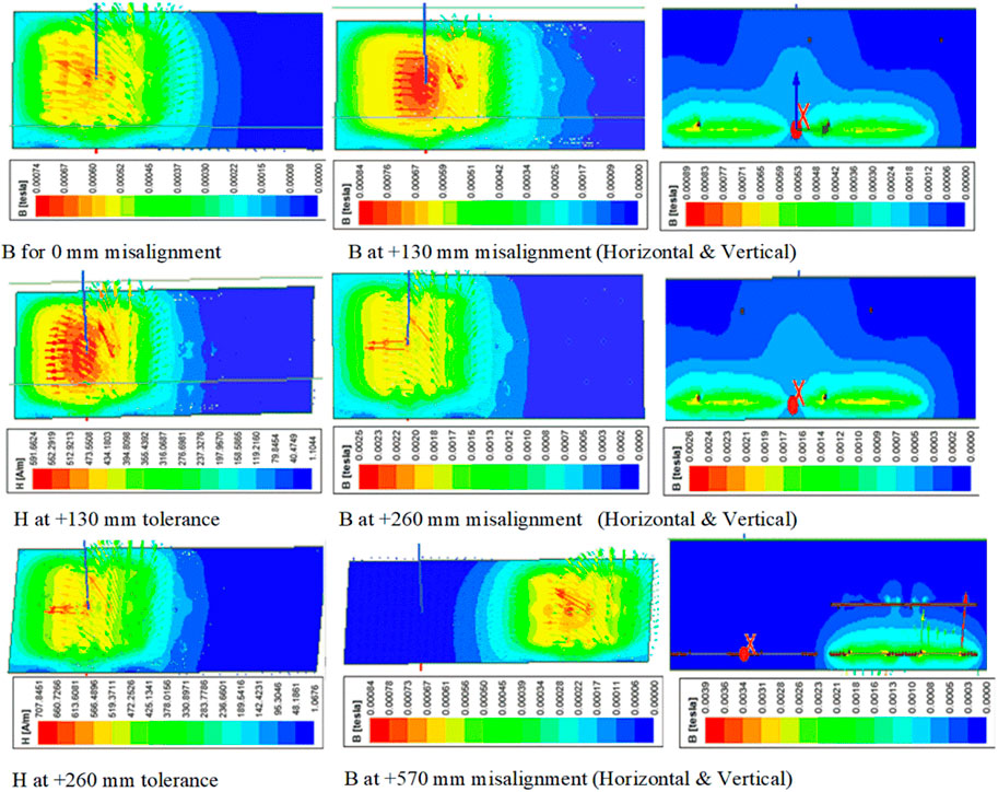
FIGURE 11. Magnetic field variations for various misalignment conditions.
The eddy current solver in ANSYS MAXWELL 3D design helped analyze the charging pads parameters. This FEA software made it simple to analyse how the mutual inductance changed concerning the distance between the pads. Mathematically, the non-linearity makes it challenging to determine the exact inductance parameters concerning the gap between the pads−the inductive parameters such as k, M, LsT, and LsR. The adjacent gap between the TPs concerning the cross-coupling inductance affects the mutual inductance. The adjacent gap of the pads relates to uniform power transfer ability analyzed with this FEA analysis software. The voltage variations across the charging pads concerning the load resistance are mentioned in Figures 12A, B. The MATLAB Simulink is used to obtain these results for the variations of k and 0C. The characteristics of the system parameters such as charging couplers’ voltage and efficiency concerning load resistance is analyzed for different k values. On the transmitter side, the voltage is increased and on the receiver side, the voltage is decreased concerning increases in load resistance.
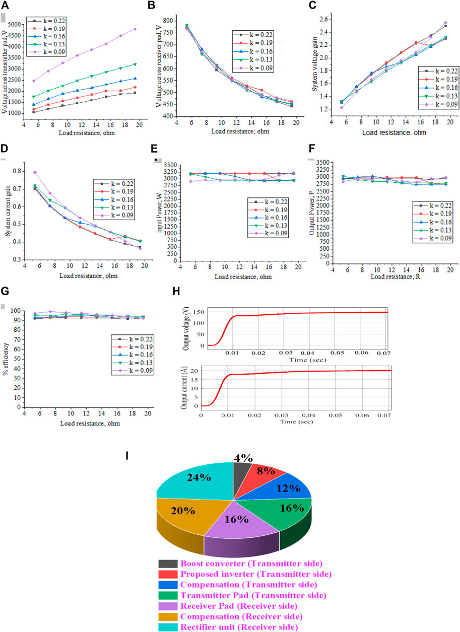
FIGURE 12. (A) RL vs. Voltage across transmitter pad (B) RL vs. Voltage across receiver pad (C) RL vs. overall system voltage gain (D) RL vs. overall system current gain (E) RL vs. input power (F) RL vs. output power (G) RL vs. %efficiency (H) Output voltage and current waveforms for k = 0.22 (I) Loss distribution of the proposed system.
The transferred power is maintained constant though the charging current and voltage varied. And it is independent of variations in load resistance. In a simulation study, to represent that the transferred power across the charging pads is constant, the battery resistance is varied. The voltage across the charging pads is indirectly proportional to the current flowing through the charging pads. The initial voltage across the transmitter pad is increased when the co-efficient of coupling decreases.
2.4.1 Loss analysis
The overall system efficiency (
The total losses of the system is obtained by calculating the losses contributed by boost converter (
The losses due to the charging pad can be calculated with the help of L, ω, a.c. resistance of the coil (rac), volt-ampere of the charging pad (Tejeda, 2018).
The losses across the any pad are given in Eq. 40)
The core loss of the charging pad for the used ferrite core is determined from Steinmetz equation, where fs is system frequency, B is flux density, and α, β, Cm is co-efficient that can be obtained by data sheet specifications.
The losses of the inverter can be obtained by calculating the switching and conduction losses of the used SiC MOSFET. Also, the losses of the diode can be calculated similarly adding those losses.
Where, Vds is commutation voltage, ton,M and toff,M are turn-on and turn-off time of the switches, Vgs and Qg are voltage and charge of gate to source terminals of the MOSFET, Irms,M is current flowing through the MOSFET, Rds(on) is on-state resistance of the MOSFET, VF and VD are forward voltage and voltage of the diode respectively, Irms,D and Iavg,D are diodes’ rms and average current respectively.
The 42 SWG, 1050 strands Litz wire is used to wound the coil. It has low skin depth and the CF29715509, 55*45*9 mm ferrite bars are used in core structure. Figure 12I represents the loss distribution of the proposed system. Eq. 37 represents the overall efficiency of the system. The 1200 V, 30 A SiC MOSFET is used in a proposed inverter, KEMET capacitors are used in compensation network. The SiC Schottky diodes are used in receiver side rectifier unit. The overall d.c.-d.c. efficiency of the system is 88% at the rated load conditions. Figure 12I represents the loss contribution of the different stages of the proposed system.
2.4.2 Response of system parameters concerning load resistance (battery equivalent resistance): Simulink analysis
The output parameters of the overall charging system are represented from 12 (c)-(h). Variations in load resistance led to a decrease in the current gain and increases in the voltage gain of the system. The load resistance represents the equivalent resistance of the battery—the maximum power transfers to the receiver from the transmitter due to the MPPT algorithm. Irrelevant of k, there is no oscillatory characteristics curve. The voltage across the transmitter pad increases linearly, and across the receiver, the pad decreases gradually, concerning increases in RL. The delivered voltage decreases, and the current increases on the inverter for RL variations. The voltage gains increase linearly, and the current gain decays rapidly. The transferred power of the system is maintained constant for the variations of k and RL. The input and output power variations concerning the k and RL are maintained constant in our developed system, and hence from Figure 12G, the system’s efficiency maintains a stable state by an algorithm. The efficiency of the simulated system varied by 90%–95% concerning the k and RL. The load resistance is set by 7.2 Ω to obtain the required 144 V and 20 A output voltage and current.
2.4.3 Hardware analysis
Figure 13 represents the hardware output waveforms of the proposed system. The 3.3 kW PV-integrated dynamic charging system provides the 20 A charging current with 88% efficiency at the rated load resistance. Concerning the load resistance variations, the output voltage and current will vary. The systems’ quality factor is 4, and the coupling coefficient is 0.22. The vertical gap of the charging coupler is 100 mm to obtain the required k value. The TPs’ self-inductance is 223.8 μH, the RPs’ self-inductance is 55.1 μH, and the corresponding mutual inductance is 55.1 μH. The ferrite bars are placed under the charging couplers to increase the magnetic flux density. Since the represented inductance parameters are inconsistent during the longitudinal misalignment. The resonant capacitors 15 nF and 66 nF are used on TP and RP sides, respectively, to achieve the resonant condition.
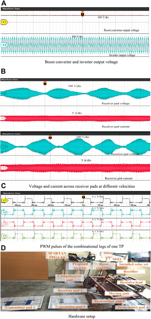
FIGURE 13. Hardware and its output waveforms. (A) Boost converter and inverter output voltage, (B) Voltage and current across receiver pads at different velocities, (C) PWM pulses of the combinational legs of one TP, (D) Hardware setup.
Additionally, the resonant network improves the power transfer profile of the proposed system. The system is designed for a load resistance of 7.2 Ω. The input and output parameters will vary concerning load resistance and input voltage. The transmitter side d.c.-d.c. converter receives the input voltage from PV arrays. The input capacitor Cin maintains the input voltage of the d.c.-d.c. converter without large variations. The charging system utilizes instant energy parameters. Since the proposed charging system is dynamic and the RP crosses the installed TPs within a particular period. 13b represents the voltage and current response of the RP for the dynamic condition. The obtained waveforms have represented the current and voltage response for the RP’s different velocities. The Figure 13C represents the combinational legs driving pulses, and the frequency of the driving pulses is 85 kHz.
3 Conclusion
The PV-integrated five-leg inverter-driven quasi-dynamic wireless charging for an electric vehicle is proposed in this paper. The paper is mainly concentrates on the five-leg inverter topology, coil pad design and renewable energy integration. The MPPT algorithm maximizes the generated power of the PV arrays. A DD coil with the exact outer dimensions is used as a receiver and transmitter to transfer the power efficiently. The proposed system maintains the efficient power transfer profile concerning the k and RL variations. The PV power is boosted up by a designed boost converter with MPPT algorithm. The series-series compensation is used to achieve the maximum power transfer profile during misalignment. However, in the real-time implementation, an energy storage system will constantly supply the wireless charging unit.
Data availability statement
The original contributions presented in the study are included in the article/supplementary material, further inquiries can be directed to the corresponding authors.
Author contributions
All authors listed have made a substantial, direct, and intellectual contribution to the work and approved it for publication.
Funding
This work was supported in part by the Government of India, Department of Science and Technology (DST) Science and Engineering Research Board (SERB) Core Research Grant CRG/2020/004073.
Conflict of interest
The authors declare that the research was conducted in the absence of any commercial or financial relationships that could be construed as a potential conflict of interest.
Publisher’s note
All claims expressed in this article are solely those of the authors and do not necessarily represent those of their affiliated organizations, or those of the publisher, the editors and the reviewers. Any product that may be evaluated in this article, or claim that may be made by its manufacturer, is not guaranteed or endorsed by the publisher.
Abbreviations
EV, Electric vehicle; DC, Direct Current; AC, Alternating Current; PV, Photo Voltaic; IPT, Inductive Power Transfer; DWPT, Dynamic Wireless Power Transfer; IMC, In-Motion Charging; DDP, Double D-pad; CP, Circular Pad; BPP, Bipolar Pad; P and O, Perturbation and Observation; MPPT, Maximum PowerPoint Tracking; PI, Proportional-Integral; KRRI, Korea Railroad Research Institute; KAIST, Korea Advanced Institute of Science and Technology; OLEV, On-Line Electric Vehicle; HPHFI, High Power High-Frequency Inverter; TP, Transmitter pad; RP, Receiver Pad; DWC, Dynamic wireless charging; SWC, Static wireless charging.
References
Aditya, K. (2016). Design and implementation of an inductive power transfer system for wireless charging of future electric transportation. e-thesis. University of Ontario Institute of Technology, Oshawa, Ontario, Canada.
Barsari, V. Z., Thrimawithana, D. J., and Covic, G. A. (2021). An inductive coupler array for in-motion wireless charging of electric vehicles. IEEE Trans. Power Electron. 36 (9), 9854–9863. doi:10.1109/TPEL.2021.3058666
Budhia, M., Boys, J. T., Covic, G. A., and Huang, C. Y. (2013). Development of a single-sided flux magnetic coupler for electric vehicle IPT charging systems. IEEE Trans. Industrial Electron. 60 (1), 318–328. doi:10.1109/TIE.2011.2179274
Celik, T., and Kusetogullari, H. (2010). Solar-powered automated road surveillance system for speed violation detection. IEEE Trans. Industrial Electron. 57 (9), 3216–3227. doi:10.1109/TIE.2009.2038395
Choi, S. Y., Gu, B. W., Jeong, S. Y., and Rim, C. T. (2015). Advances in wireless power transfer systems for roadway-powered electric vehicles. IEEE J. Emerg. Sel. Top. Power Electron. 3 (1), 18–36. doi:10.1109/JESTPE.2014.2343674
Dai, X., Jiang, J. C., and Wu, J. Q. (2019). Charging area determining and power enhancement method for multiexcitation unit configuration of wirelessly dynamic charging EV system. IEEE Trans. Industrial Electron. 66 (5), 4086–4096. doi:10.1109/TIE.2018.2860537
Farajizadeh, F., Vilathgamuwa, D. M., Jovanovic, D., Jayathurathnage, P., Ledwich, G., and Madawala, U. (2020). Expandable N-legged converter to drive closely spaced multitransmitter wireless power transfer systems for dynamic charging. IEEE Trans. Power Electron. 35 (4), 3794–3806. doi:10.1109/TPEL.2019.2939848
Greenhouse, H. (1974). Design of planar rectangular microelectronic inductors. IEEE Trans. Parts, Hybrids, Packag. 10, 101–109. doi:10.1109/TPHP.1974.1134841
Grover, F. W.Instrument Society of America (1981). Inductance calculations: Working formulas and tables. New York: Instrument Society of America.
He, H., Liu, Y., Wei, B., Wu, X., Jiang, B., and Wei, C. (2021). “Efficiency improvement for multi-parallel inverters IPT system in wide power range,” in Peas 2021 - 2021 IEEE 1st international power electronics and application symposium, conference proceeding. doi:10.1109/PEAS53589.2021.9628741
Hohm, D. P., and Ropp, M. E. (2000). “Comparative study of maximum power point tracking algorithms using an experimental, programmable, maximum power point tracking test bed,” in Conference record of the IEEE photovoltaic specialists conference, 1699–1702. doi:10.1109/PVSC.2000.916230
Huang, Z., Iam, I. W., Hoi, I. U., Lam, C.-S., Mak, P.-I., and Martins, R. P. (2019). “Self-contained solar-powered inductive power transfer system for wireless electric vehicle charging,” in 2019 IEEE PES Asia-Pacific Power and Energy Engineering Conference (APPEEC), Macao, China, 2019, 1–6. doi:10.1109/APPEEC45492.2019.8994554
Indian highway to host 250 MW solar plant – pv magazine International (2022). Indian highway to host 250 MW solar plant – pv magazine International. Available at: https://www.pv-magazine.com/2021/06/08/indian-highway-to-host-250-mw-solar-plant/ (Accessed May 16, 2022).
Kim, J. H., Lee, B. S., Lee, J. H., Lee, S. H., Park, C. B., Jung, S. M., et al. (2015). Development of 1-MW inductive power transfer system for a high-speed train. IEEE Trans. Industrial Electron. 62 (10), 6242–6250. doi:10.1109/TIE.2015.2417122
Koutroulis, E., Kalaitzakis, K., and Voulgaris, N. C. (2001). Development of a microcontroller-based, photovoltaic maximum power point tracking control system. IEEE Trans. Power Electron. 16 (1), 46–54. doi:10.1109/63.903988
Laporte, S., Coquery, G., Deniau, V., de Bernardinis, A., and Hautière, N. (2019). Dynamicwireless power transfer charging infrastructure for future evs: From experimental track to real circulated roads demonstrations. World Electr. Veh. J. 10 (4), 84. doi:10.3390/wevj10040084
Lee, E. S., Kim, M. Y., Kang, S. M., and Han, S. H. (2022). Segmented IPT coil design for continuous multiple charging of an electrified monorail system. IEEE Trans. Power Electron. 37 (3), 3636–3649. doi:10.1109/TPEL.2021.3115511
Liu, J., Liu, Z., Chen, W., Sun, X., and Su, H. (2022). An optimized coil array and passivity-based control for receiving side multilevel connected D.C.-D.C. Converter of dynamic wireless charging. IEEE Trans. Veh. Technol. 71 (4), 3715–3726. doi:10.1109/TVT.2022.3146636
Mahesh, A., Chokkalingam, B., and Mihet-Popa, L. (2021). Inductive wireless power transfer charging for electric vehicles-A review. IEEE Access 9, 137667–137713. doi:10.1109/ACCESS.2021.3116678
Mohamed, A. T., Mahmoud, M. F., Swief, R. A., Said, L. A., and Radwan, A. G. (2021). Optimal fractional-order PI with D.C.-D.C. converter and PV system. Ain Shams Eng. J. 12 (2), 1895–1906. doi:10.1016/J.ASEJ.2021.01.005
Mouli, G. R. C., van Duijsen, P., Grazian, F., Jamodkar, A., Bauer, P., and Isabella, O. (2020). Sustainable e-bike charging station that enables ac, d.c. andwireless charging from solar energy. Energies 13 (14), 3549. doi:10.3390/en13143549
Narayanamoorthi, R., and Juliet, A. V. (2019). Capacitor-less high-strength resonant wireless power transfer using open bifilar spiral coil. IEEE Trans. Appl. Supercond. 29 (1), 1–8. doi:10.1109/TASC.2018.2848268
Narayanamoorthi, R., Vimala Juliet, A., and Chokkalingam, B. (2019). Cross interference minimization and simultaneous wireless power transfer to multiple frequency loads using frequency bifurcation approach. IEEE Trans. Power Electron. 34 (11), 10898–10909. doi:10.1109/TPEL.2019.2898453
Ombach, G., Kurschner, D., Mathar, S., and Chlebosz, W. (2015). “Optimum magnetic solution for interoperable system for stationary wireless EV charging,” in 2015 10th international conference on ecological vehicles and renewable energies. EVER 2015. doi:10.1109/EVER.2015.7112996
Patil, D., McDonough, M. K., Miller, J. M., Fahimi, B., and Balsara, P. T. (2017). Wireless power transfer for vehicular applications: Overview and challenges. IEEE Trans. Transp. Electrification 4 (1), 3–37. doi:10.1109/TTE.2017.2780627
Rahulkumar, J., Narayanamoorthi, R., Vishnuram, P., Bajaj, M., Blazek, V., Prokop, L., et al. (2022). An empirical survey on wireless inductive power pad and resonant magnetic field coupling for in-motion EV charging system. IEEE Access 11, 4660–4693. doi:10.1109/ACCESS.2022.3232852
Rashid, M. H. (2004). Power electronics: Devices, circuits, and applications. 3rd edition. Pearson/Prentice Hall, ISBN: 9780131011403.
RosaE. B.GroverF. W. (n. d.). “Formulas and tables for the calculation of mutual and self-inductance (Revised),” in Bulletin of the Bureau of Standards 8: 1.
SAE International (2020). Wireless power transfer for light-duty plug-in/electric vehicles and alignment methodology J2954_202010.
Shanmugam, Y., Narayanamoorthi, R., Vishnuram, P., Bajaj, M., Aboras, K. M., Thakur, P., et al. (2022). A systematic review of dynamic wireless charging system for electric transportation. IEEE Access 10, 133617–133642. 1. doi:10.1109/ACCESS.2022.3227217
Shevchenko, V., Husev, O., Strzelecki, R., Pakhaliuk, B., Poliakov, N., and Strzelecka, N. (2019). Compensation topologies in IPT systems: Standards, requirements, classification, analysis, comparison and application. IEEE Access 7, 120559–120580. doi:10.1109/ACCESS.2019.2937891
Shin, J., Shin, S., Kim, Y., Ahn, S., Lee, S., Jung, G., et al. (2014). Design and implementation of shaped magnetic-resonance-based wireless power transfer system for roadway-powered moving electric vehicles. IEEE Trans. Industrial Electron. 61 (3), 1179–1192. doi:10.1109/TIE.2013.2258294
Singaravel, M. M. R., and Daniel, S. A. (2015). MPPT with single D.C.-D.C. Converter and inverter for grid-connected hybrid wind-driven PMSG-PV system. IEEE Trans. Industrial Electron. 62 (8), 4849–4857. doi:10.1109/TIE.2015.2399277
Tejeda, A. (2018). Development of new magnetic couplers for wireless charging of electric vehicles. e-thesis. Department of electrical and computer engineering, The University of Auckland, New Zealand.
The Global Electric Vehicle Market In 2022 – Virta (2022). The global electric vehicle market in 2022-Virta. Available at: https://www.virta.global/global-electric-vehicle-market?__hstc=51530422.a4119e1ebb088c79a85539e9c7f610ae.1651463928498.1651463928498.1651463928498.1&__hssc=51530422.1.1651463928499&__hsfp=3432168314&hsutk=a4119e1ebb088c79a85539e9c7f610ae&contentType=standard-page#six (Accessed May 13, 2022).
The Paris Agreement | United Nations (2022). The Paris agreement | united Nations. Available at: https://www.un.org/en/climatechange/paris-agreement (Accessed May 13, 2022).
UmanandL. (2009). Power electronics essentials and applications. Wiley India Pvt. Limited ISBN:9788126519453
Vu, V. B., Phan, V. T., Dahidah, M., and Pickert, V. (2019). Multiple output inductive charger for electric vehicles. IEEE Trans. Power Electron. 34 (8), 7350–7368. doi:10.1109/TPEL.2018.2882945
Yang, G., Song, K., Sun, Y., Huang, X., Li, J., Guo, Y., et al. (2021). Interoperability improvement for rectangular pad and DD pad of wireless electric vehicle charging system based on adaptive position adjustment. IEEE Trans. Industry Appl. 57 (3), 2613–2624. doi:10.1109/TIA.2021.3056639
Yuvaraja, S., Narayanamoorthi, R., Sathik Mohamed Ali, J., and Almakhles, D. (2022). A comprehensive review of the on-road wireless charging system for E-mobility applications. Front. Energy Res. 10. doi:10.3389/fenrg.2022.926270
Zaheer, A., Neath, M., Beh, H. Z., and Covic, G. A. (2017). A dynamic EV charging system for slow moving traffic applications. IEEE Trans. Transp. Electrification 3 (2), 354–369. doi:10.1109/TTE.2016.2628796
Zhou, B., Pei, J., Calautit, J. K., Zhang, J., and Guo, F. (2021). Solar self-powered wireless charging pavement—A review on photovoltaic pavement and wireless charging for electric vehicles. Sustain. Energy Fuels 5 (20), 5139–5159. doi:10.1039/d1se00739d
“Arena del Futuro” Demonstrates Capability of Dynamic Inductive Recharging Technology for Electric Vehicles | Stellantis (2022). Demonstrates capability of dynamic inductive recharging technology for electric vehicles. Available at: https://www.stellantis.com/en/news/press-releases/2022/june/arena-del-futuro-demonstrates-capability-of-dynamic-inductive-recharging-technology-for-electric-vehicles?adobe_mc_ref= (Accessed June 16, 2022).
Keywords: dynamic wireless power transfer, electric vehicle charging, power converters, wireless charging coil, inductive coupling
Citation: Shanmugam Y, Narayanamoorthi R, Vishnuram P, Savio D, Yadav A, Bajaj M, Nauman A, Khurshaid T and Kamel S (2023) Solar-powered five-leg inverter-driven quasi-dynamic charging for a slow-moving vehicle. Front. Energy Res. 11:1115262. doi: 10.3389/fenrg.2023.1115262
Received: 03 December 2022; Accepted: 27 February 2023;
Published: 09 March 2023.
Edited by:
Dongran Song, Central South University, ChinaReviewed by:
Zhi Zhang, Dongguan University of Technology, ChinaDeepa Kaliyaperumal, Amrita Vishwa Vidyapeetham, India
Copyright © 2023 Shanmugam, Narayanamoorthi, Vishnuram, Savio, Yadav, Bajaj, Nauman, Khurshaid and Kamel. This is an open-access article distributed under the terms of the Creative Commons Attribution License (CC BY). The use, distribution or reproduction in other forums is permitted, provided the original author(s) and the copyright owner(s) are credited and that the original publication in this journal is cited, in accordance with accepted academic practice. No use, distribution or reproduction is permitted which does not comply with these terms.
*Correspondence: R. Narayanamoorthi, narayanamoorthi.r@gmail.com; Mohit Bajaj, thebestbajaj@gmail.com; Ali Nauman, anauman@ynu.ac.kr; Tahir Khurshaid, tahir@ynu.ac.kr; Salah Kamel, skamel@aswu.edu.eg